A World of Chips Acts: The Future of U.S. – E.U. Semiconductor Collaboration
CSIS
By Sujai Shivakumar, Charles Wessner, and Thomas Howell
August 20, 2024
The United States and the European Union have each recently enacted legislation providing for an unprecedented volume of public investments in semiconductors, with the largest portion allocated to the establishment of new onshore chip production facilities. Substantial funds are also allocated to semiconductor research and development, supply chain security, and workforce expansion and training. These parallel initiatives have been prompted by an awareness in both regions of threats to economic and strategic security arising out of their dependency on foreign-made chips. The question posed by the enactment of the two Chips Acts is how such joint activities can be deepened, broadened, and leveraged by direct engagement between the United States, the European Union, and national authorities to address the vulnerabilities faced by both ecosystems.
Shared Vulnerabilities
Both the U.S. and EU economies were disrupted by shortages of semiconductors during the Covid-19 pandemic. These emerged from unexpected surges in demand for chips (e.g., for electronic devices), which led to curtailed auto production in both regions. Reportedly, the U.S. automotive industry lost production of some four million vehicles due to chip shortages in and after 2020, while in Europe, a senior German official observed in 2023 that “we lost 1-1.5 percent of our GDP in 2021 because of a lack of semiconductors—or about €40bn.”
Genuine post-pandemic vulnerabilities remain. Both the United States and the European Union are heavily dependent on chips fabricated in Taiwan and could experience catastrophic economic disruption if conflict between China and Taiwan shuts off the island’s semiconductor exports. Arati Prabhakar, director of the White House Office of Science and Technology Policy, said in January 2024 that “all of the leading-edge chips that are critical to our infrastructure, to AI, to our national security ambitions, automotive manufacturing even, are being built in one part—a fragile part of the world [Taiwan].” Bloomberg Economics estimates that a war over Taiwan would cost the global economy $10 trillion in the first year. While this may overstate the risk, even a fraction of that loss would be devastating.
The United States and the European Union share the reality that neither party has the capability to manufacture at scale the most advanced semiconductors, which are at the 2 and 3 nanometer (nm) nodes. That capability resides in part in South Korea but mainly in Taiwan. These chips are essential to produce new generations of advanced artificial intelligence (AI) as well as for 5G and 6G telecommunications, applications increasingly vital to national security and economic competitiveness. Efforts to catch up with the leaders in the production of the most advanced logic chips and to establish secure chip supply chains will require very large and sustained investments and significant technological effort. With the United States and the European Union facing the same strategic dilemma and seeking to avoid costly duplicative investments, it is not surprising that both Chips Acts call for international collaboration with allies and partners. (The U.S. CHIPS Act is an acronym: Creating Helpful Incentives to Produce Semiconductors. The EU Chips Act is not. When referring to them together, the authors have opted for Chips Acts. When referred to separately, they are referred to as U.S. CHIPS and EU Chips.)
To be sure, U.S.- and EU-based chip companies have decades of experience collaborating on chip research and production at universities and research organizations such as France’s CEA-Leti, Belgium’s Imec, and the Albany NanoTech Complex. Companies based in the United States and Europe have operated chipmaking facilities and participated in collaborative research centers for many years.
With the United States and the European Union facing the same strategic dilemma and seeking to avoid costly duplicative investments, it is not surprising that both Chips Acts call for international collaboration with allies and partners.
Comparing the U.S. and EU Chips Acts
The broad outlines of the U.S. and EU Chips Acts are similar, reflecting shared concerns. It is clear that, as the two acts were in their formative stages, each party took note of the measures being contemplated by the other.
Both pieces of legislation envision industry-government partnerships with similar strategic goals: reducing dependency on offshore chip manufacturing, ensuring greater supply chain security and resiliency, encouraging production at the leading edge, and growing a workforce to support the achievement of these goals.
The amount of direct public funding provided pursuant to both acts is roughly comparable. Each party allocates the bulk of the planned expenditure to investments in onshore chipmaking facilities. Most of the remainder will be directed toward applied R&D by public-private research organizations to enable “lab-to-fab” transfers of innovations from the research base to industry.
Both acts emerged as policy responses to the geostrategic risks and eventual technological challenge of a rising China, compounded by the concentration of the world’s most advanced semiconductor production being in Taiwan, with its geostrategic and geological risks.
Both the United States and the European Union acknowledge that existing interdependencies between them make collaboration imperative. Reflecting that awareness, EU-based semiconductor firms are eligible for U.S. CHIPS Act funding and U.S.-based firms can receive EU Chips Act support.
Both parties are in accord that Japan must be involved in Chips Act–related initiatives, reflecting its “like-minded” democracy status and its dominance in many key semiconductor equipment and materials sectors. Importantly, Japan has recently launched a major initiative: Rapidus, a government-funded start-up foundry that is working in close cooperation with New York CREATES at the Albany Nanotech Complex and Belgium’s Imec with ambitions to regain Japan’s place at the forefront of global advanced chip production.
While they have similar objectives, the U.S. and EU Chips Acts are distinguishable in a number of respects:
State Aid Issues: European Union competition law provides that “state aids” (subsidies) are prohibited unless approved by EU competition authorities pursuant to one of the exceptions to the general prohibition, such as aids for regional development, environmental and climate purposes, or research and innovation. The EU Chips Act’s public outlays by member states are subject to this approval requirement. In order to fit within one of the exceptions to the state aids prohibition, EU Chips Act funds must be directed to “first-of-kind” manufacturing facilities that fall under the exception for promotion of innovation (or other exceptions, such as regional development). The United States has no comparable rule or law limiting “state aids” or subjecting subsidies by U.S. states to prior federal approval.
Federal and State-Based Support: U.S. federal CHIPS Act subsidies are augmenting state government incentives for chip facilities, some of which are substantial—New York State, for example, is providing Micron Technologies $5.5 billion to support its investment in two new memory chip fabs near Syracuse. In contrast to the European Union, which must approve all state aid initiatives, the federal government lacks the authority to regulate such state outlays, leading some observers to warn of a subsidy race among U.S. states. It is worth noting, though, that in reality such subsidy races have existed among U.S. states and foreign governments for decades.
New vs. Existing Funding: A major difference is that “the EU Chips Act does not create new financial resources.” The U.S. CHIPS Act funding is “new money”—federal outlays appropriated by Congress for the first time. EU Chips Act expenditures consist primarily of funds being redirected from existing EU-funded programs, although within individual member states new funds seem to be available. Still, the European Commission is allocating €4.2 billion from its budget to implement the research elements of the Chips Act; of this, €2.7 billion is being redirected from Horizon Europe, the European Union’s umbrella research and innovation program, and €1.4 billion from the Digital Europe Program, which seeks to encourage the use of digital technologies by European businesses and public institutions. This “shuffling of funds” between EU programs is proving controversial. According to one member of the European Parliament, the result is “a shame for Europe because we are investing in chips, but we take it away from other priorities like cybersecurity. We trade our future against our security.” A European academic recently fumed that “Horizon Europe is not a lemon, so stop squeezing it.”
Tax Incentives: In a major difference, the U.S. CHIPS Act provides substantial new federal tax incentives for investments in chipmaking facilities, while the EU Chips Act does not. The U.S. tax incentives are generous, providing up to 25 percent tax credits for investments initiated (not completed) by the end of 2026.
Different Frameworks: The institutional framework for most U.S. CHIPS Act funding is relatively simple: a bilateral grant agreement between the Department of Commerce and individual industry recipients. The EU Chips Act has more layers and more players. Companies seeking public funding must first secure commitments from one or more individual member state governments, but those outlays must be approved by the European Commission pursuant to the EU competition rules. The EU Chips Act provisions for applied research emphasize public-private consortia involving multiple industrial and public actors and multiple member states. The U.S. programs are more straightforward, but some critics have suggested that they include a multiplicity of requirements that add complications in process and execution. The U.S. CHIPS Act also has “upside sharing” provisions which require firms receiving $150 million or more in federal funding which subsequently enjoy windfall profits to share a portion of their future returns above an established threshold. The government will use moneys received to support the purposes of the CHIPS Act.
Regulatory Issues: The EU Chips Act contains a provision to expedite the permitting process for first-of-kind chip facilities, even to the extent of allowing derogation from environmental requirements. The U.S. CHIPS Act has no comparable provision (although it is likely to need one). U.S. chipmaking facilities could be delayed for several years if the National Environmental Policy Act is allowed to apply to planned greenfield chipmaking facilities.
Synopsis of the U.S. CHIPS Act
The U.S. CHIPS and Science Act of 2022 was enacted in August 2022, though the “CHIPS Act” incentives and research programs were initially established (unfunded) in the National Defense Authorization Act for Fiscal Year 2021.
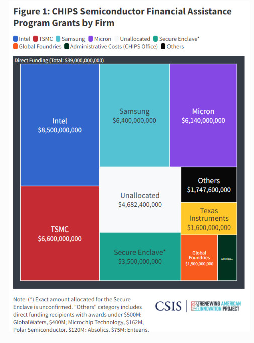
The CHIPS Act authorized and appropriated $39 billion in grants, loans, and loan guarantees for chip manufacturing on U.S. soil.
The CHIPS Act provided a 25 percent tax credit, initially valued by the Congressional Budget Office at $46 billion, for investments in chip manufacturing facilities.
The CHIPS Act appropriated $2 billion for the Department of Defense (DOD) Microelectronics Commons, along with $11 billion for Department of Commerce research and development programs. This included the establishment of a National Semiconductor Technology Center (NSTC), a National Advanced Packaging Manufacturing Program (NAPMP), a Manufacturing USA Institute, and funding for related National Institute of Standards and Technology (NIST) microelectronics research.
Another $2 billion was initially set aside for legacy chips used in automotive and many other applications, though NIST sees the $2 billion figure as “a floor, not a ceiling.”
Companies awarded subsidies under the CHIPS Act are subject to a 10-year ban prohibiting them from producing chips at nodes under 28 nanometers in China, Russia, and other “countries of concern.”
The CHIPS Act also authorized, but did not appropriate, $174 billion for various federal science and research programs not directly focused on semiconductors and telecommunications.
Governance Structure
President Biden and the Department of Commerce have taken a number of institutional steps to ensure the implementation of the CHIPS Act:
- The White House, pursuant to the CHIPS Act, has established a Subcommittee for Microelectronics Leadership within the President’s National Science and Technology Council. The subcommittee is tasked with developing a national strategy for microelectronics research, development, manufacturing, and supply chain security.
- The White House has established the CHIPS Innovation Steering Council to “coordinate and develop the policies needed to effectively implement the [CHIPS] Act within the executive branch.”
- The Commerce Department has established two offices within NIST:
-
- The CHIPS Program Office (CPO) is tasked with awarding CHIPS Act funding, engaging stakeholders, and coordinating semiconductor-related activities of the federal agencies. At the end of November 2023, Adrienne Elrod, director of external and government affairs at CPO, reported that CPO had hired over 150 staffers; as of July 2024, it had received over 670 expressions of interest from semiconductor firms proposing investments in chips research, production, and construction of facilities.
- The CHIPS R&D Office is to oversee the NSTC, the NAPMP, the CHIPS Manufacturing USA Institute, and CHIPS metrology research, receiving advisory support from an Industrial Advisory Committee staffed with industry and academic experts in microelectronics fields.
- Importantly, the two offices are to jointly engage with comparable organizations in allied and partner countries.
Implementation to Date
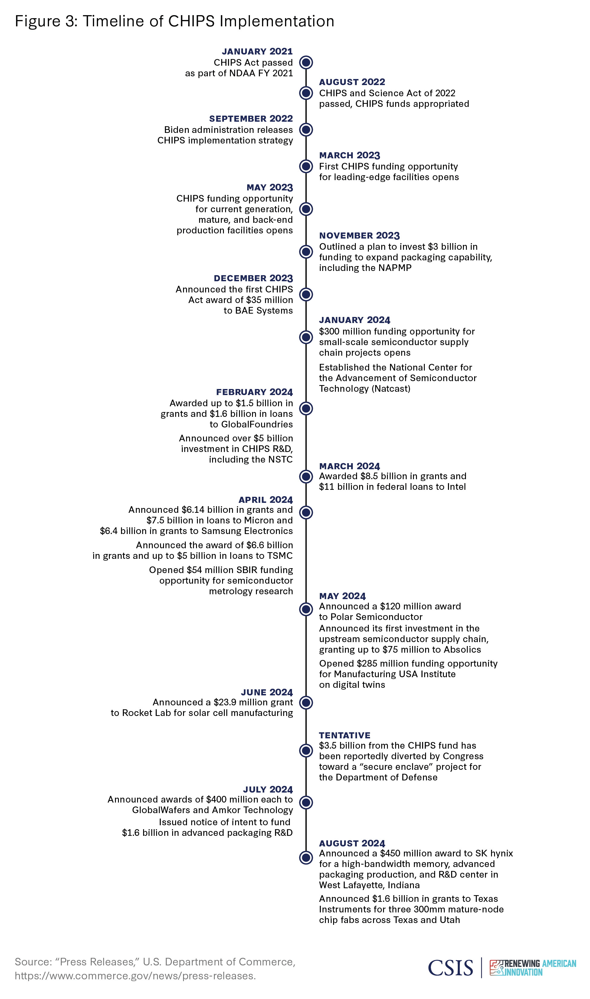
Some observers have criticized the slow pace at which the CHIPS Act has been implemented without regard for the novelty and scale of the program, but in late 2023 and throughout 2024 the Commerce Department made a flurry of major awards:
- On December 11, 2023, the Commerce Department announced its first CHIPS Act award, a grant of $35 million to the UK-based BAE Systems to quadruple its capacity for making specialized devices for use in F-15 and F-35 fighter jets, satellites, and other defense systems.
- In January 2024, the Commerce Department announced a CHIPS Act award of $162 million to Microchip Technology, intended to significantly increase its production of microcontrollers and mature-node semiconductors with applications in automobiles, cellphones, and the defense and aerospace sectors. The funds will be used to triple the capacity of the company’s fabrication sites in Colorado and Oregon.
- In January 2024, Secretary of Commerce Gina Raimondo announced the creation of the National Center for the Advancement of Semiconductor Technology (Natcast), a nonprofit tasked with operating the NSTC, which will be the “focal point for research and engineering throughout the semiconductor ecosystem.”
- As noted, in November 2023, the Commerce Department outlined a plan to invest $3 billion in CHIPS Act funds to expand U.S. advanced packaging capability. The department noted that at present, “we do not have advanced packaging in the US capable of high-volume manufacturing.” The advanced packaging plan will include a pilot facility that will “provide a place to test the new equipment and processes” and “allow for hands-on workforce development.”
- Throughout 2024, the Commerce Department announced the award of multi-billion-dollar incentive packages to major chip manufacturers for investments in wafer fabrication facilities in the United States:
-
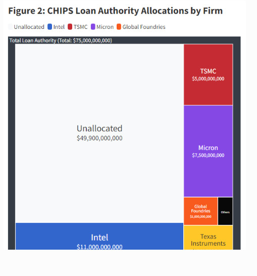
- In February, CHIPS awarded GlobalFoundries up to $1.5 billion and $1.6 billion in loans, respectively, to expand its campus in Malta, New York, and to revitalize its fabrication plant in Burlington, Vermont.
- In March, the Commerce Department announced the award of $8.5 billion in grants to Intel Corporation, making available up to $11 billion in federal loans. Intel indicated it would use the support for investments in Ohio, Arizona, New Mexico, and Oregon.
- In April, the Commerce Department announced the award of $6.14 billion in grants to Micron Technology for investments in two semiconductor memory facilities in Syracuse, New York, as well a third fab colocated with its existing facility in Boise, Idaho.
- That same month, the Commerce Department announced the award of $6.6 billion in grants and up to $5 billion in loans to Taiwan Semiconductor Manufacturing Company (TSMC) to build a third chip fabrication facility in addition to its two facilities under construction in Arizona. The newest fab will reportedly manufacture chips at process technologies of 2 nm or below.
- The Commerce Department also awarded $6.4 billion to Samsung Electronics to support its investments in a new chipmaking campus in Taylor, Texas, as well as an expansion of its Austin, Texas facilities.
- In May, the Commerce Department awarded $120 million to Polar Semiconductor, a maker of power and sensor chips, to double its U.S. production capacity in Minnesota. The deal will allow Polar to draw in another $450 million in U.S. private capital and $75 million from the state of Minnesota, helping to transform Polar to a majority U.S.-owned foundry.
- In May, the Commerce Department announced its first investment in the upstream semiconductor supply chain, granting up to $75 million to Absolics for a facility manufacturing next-generation glass substrates in Covington, Georgia.
- Although unconfirmed, according to Politico, $3.5 billion from the CHIPS fund has been reportedly diverted toward a “secure enclave” project to manufacture state-of-the-art and secure chips for defense purposes. Draft appropriations legislation passed by the House Committee on Appropriations shows $1.5 billion allocated for the secure enclave in FY 2025.
- A May 2024 study by the Semiconductor Industry Association and the Boston Consulting Group forecast that with the CHIPS Act support, U.S.-based semiconductor capacity will increase by 203 percent by 2032, and that the U.S. share of global chipmaking capacity will increase for the first time in decades during the same time frame, from 10 percent to 14 percent.
- In June 2024, Mike Schmidt, director of the CHIPS Program Office, said that “because of the CHIPS Act, every company capable of producing leading edge semiconductors at scale is now expanding in the United States . . .”
- In July 2024, the administration announced that it was launching a “workforce partner alliance,” allocating some of the funds appropriated for the NSTC to award grants to as many as 10 workforce development projects with budgets ranging from $500,000 to $2 million.
- That same month, the CHIPS Office announced it would make several awards of roughly $150 million each, up to $1.6 billion total, for research activities to “establish and accelerate domestic capacity for semiconductor advanced packaging.”
In August 2024, the Commerce Department reached a $450 million grant agreement with South Korean advanced memory chip firm SK Hynix to support their planned $4 billion high-bandwidth memory production, packaging, and R&D hub colocated with Purdue University in West Lafayette. With this award, all five of the world’s leading-edge memory, logic, and packaging companies have now agreed to build in the United States.
DARPA’s Initiative
Federal support for the semiconductor industry pursuant to the CHIPS Act will be augmented by activities at the Defense Advanced Research Projects Agency (DARPA), funded through the DOD’s budget rather than the CHIPS Act. DARPA plans to launch a domestic hub for prototyping advanced semiconductor fabrication techniques. Given DARPA’s extraordinary track record of breakthrough innovations, this development is significant, but its impact is likely to be felt only over the longer term.
The research center envisioned by DARPA will focus on 3D heterogeneous integrated (3DHI) microsystems, which feature the integration of diverse chip types into a single package for dramatically improved performance. DARPA regards this effort as potentially transformational for the U.S. economy and hopes to stand up the center by 2029. DARPA is establishing teams via a contract to pursue the initiative in two phases, each with a projected budget of $420 million. The goal is to create “a self-sustaining 3DHI center at an existing facility that is owned and operated by a non-federal entity, and accessible to users in academia, government, and industry.”
The 3D projects bolster DARPA’s Electronics Resurgence Initiative (ERI)—launched in 2017, with a follow-on ERI 2.0 announced in 2022—which is focusing on advanced manufacturing opportunities and enabling electronic systems to function in extreme environments. DARPA plans to spend $3 billion on this effort over the next five years. DARPA’s Beyond Scaling Initiative, launched in 2017, develops software to automate and optimize chip design.
Perhaps what is most significant about the DARPA initiatives is that they underscore that the CHIPS Act, while remarkable, will not be sufficient on its own to reinvigorate and grow this key industry in the United States. The U.S. effort needs to be sustained and at scale if it is to have the desired impact, particularly in light of other countries’ sizeable investments.
Synopsis of the EU Chips Act
Arguably one major impact of the U.S. CHIPS Act was to stimulate a similar effort in Europe. The European Commission and European Parliament approved the European Chips Act in July 2023, with the act becoming effective on September 21, 2023.
As noted above, the EU Chips Act involves at least €43 billion in identified public funding, with the expectation that this will spur a roughly equal amount of private investment. Most of the public funding will be provided by the governments of the member states, not through the commission.
According to the European Union, the €43 billion in public funds will include some private money and only €3.3 billion from the European Union’s budget, making the composition of the Chips Act funding less distinct. A 2023 analysis of the Chips Act conducted under the auspices of the Austrian government laments that “it is difficult to understand who is funding what, and how much fresh money is available for the Chips Act . . . the Chips Act is to be supported with an estimated overall level of policy-driven investment in excess of EUR 43 billion up to 2030. However, it remains unclear how much will come from the EU level, Member States and companies.”
The EU Chips Act is designed to ensure Europe’s “strategic autonomy” and sovereignty by enabling a secure supply of critical chips. To do this, the European Union is creating three “pillars”:
- The Joint Undertaking: The first pillar is a public-private collaboration designated as the EU Chips Joint Undertaking (JU). It focuses on developing advanced chip technology (2 nm and below, quantum chips, and new production methods for such technologies). Themes include semiconductor research, pilot lines, standards, certification for energy efficiency and security of chips, skills, and networking of semiconductor research centers. Pillar one will reportedly be publicly funded with €11 billion. This effort roughly corresponds to the U.S. plan for the NSTC.
- Support Advanced Chip Production in Europe: The second pillar, which is to absorb the bulk of EU public funding, will seek to establish vertically integrated manufacturing centers and “open EU foundries,” which will produce chips designed by others for third parties. To qualify, projects must be “first-of-kind” in the European Union, involving novel technology nodes, substrate materials, or other innovations that enhance chip performance, such as reduced power requirements and durability. Participating second-pillar companies will receive priority access to the pilot lines established pursuant to the first pillar. Companies participating in the second pillar are eligible for financial support from the European Union and member states, with funding reportedly totaling some $30 billion. Companies like Infineon and STMicro as well as Intel are seeking a portion of these funds to support new facilities.
- Monitoring Supply: The third pillar will seek to ensure continuity of supply in the event of a chip shortage. It will involve monitoring to provide early warning of looming shortages, coordinated procurement, and a mandatory shift in production toward scarce chip types, with favorable investment terms offered to companies as a quid pro quo.
Governance of the EU Chips Act will be divided between the European Semiconductor Board and the Chips Joint Undertaking. The board will comprise representatives of the member states and be chaired by the European Commission. The Governing Board of the Chips Joint Undertaking consists of representatives from participating member states, corporate representatives, and the European Commission. Within the commission, the Chips Act is the responsibility of the Directorate-General for Communications Networks, Content, and Technology (DG-CNET).
Implementation to Date
Europe is making impressive progress with multiple major announcements. As in the United States, the prospect of public funding is having a major catalytic impact. It is also evident from investment announcements and approvals granted by the European Union and member states that implementation of the EU Chips Act will entail major collaborations with foreign partners, notably U.S. firms but also Taiwan’s TSMC.
- A leading example is U.S.-based Intel, which has outlined its plan to invest $88 billion in expanding its chip research and manufacturing facilities in Europe. In 2023, Intel secured a commitment from the government of Germany for nearly $11 billion in subsidies, which will be used to fund a chipmaking facility in Magdeburg. For its part, Intel will invest €30 billion in this project. Intel will invest €12 billion in Leixlip, Ireland, to double its manufacturing space for Intel 4 process technology. In addition, Intel is investing $4.6 billion in an assembly and test facility in Poland, which will test Intel chips fabricated in Germany and Ireland. The Polish government is expected to cover about one-third of this investment. Intel is also investing in other chip projects in France, Italy, and Spain.
- In a cooperative effort, U.S.-based GlobalFoundries and STMicroelectronics have secured approval from the European Union to receive French government subsidies to build a chip fabrication plant in Crolles, France. The French will provide $8.13 billion to this project. GlobalFoundries is also investing in the expansion of its existing facilities in Dresden, Germany.
- U.S.-based chipmaker Wolfspeed has announced plans to invest $3 billion in a new silicon carbide chip plant in Germany and expects the German government to provide 20 percent of this amount in subsidies to support the project.
- In August 2023, Infineon (Germany), Bosch (Germany), TSMC (Taiwan), and NXP Semiconductors (the Netherlands) announced plans to establish the European Semiconductor Manufacturing Company to build a chip fabrication plant in Dresden that will be majority-owned and operated by TSMC. Total investments are expected to be €10 billion and receive “strong support” from the European Union and the German government.
- In 2023, Germany’s Infineon announced plans to build a €5 billion semiconductor manufacturing facility in Dresden to make power semiconductors and analog and mixed signals components. It is seeking €1 billion in public funding to support the project.
- The European Union has approved grants of €292.5 million from the government of Italy to STMicroelectronics to build a silicon carbide semiconductor substrate manufacturing plant in Catania. In July 2024, the Chips JU announced the availability of €325 million in calling for proposals for chips research, including the creation of “competence centers” to provide technical expertise and research support, particularly for small and medium enterprises.
Government-to-Government Bilateral Engagement
Both the U.S. and the EU Chips Acts mandate international collaboration, a recognition that neither region can achieve self-sufficiency in microelectronics. While the precise form such collaboration will take is not clear, certain broad themes have begun to emerge.
Alignment of Export Controls: The United States and the European Union are taking concrete steps to align their chip technology export controls with respect to “countries of concern,” principally China. The U.S. Department of Commerce has imposed strict controls on the export of U.S. chips and chipmaking technology to China. In September 2023, the government of the Netherlands established new export licensing rules which will prevent the Dutch maker of extreme ultraviolet lithography equipment from exporting its most advanced chipmaking tools and technology to China. The European Union has released a white paper that proposes to establish a system of export controls at the EU level, as opposed to the current patchwork regime in which member states unilaterally implement their own controls.
Support for Multilateral Efforts: The U.S. CHIPS Act creates a $500 million International Technology Security and Innovation Fund administered by the State Department to support the coordination of chip export controls between the United States and its allies and partners. Participation in the fund is contingent on countries “having export controls on semiconductor trade with China that are ‘substantially equivalent’ to those imposed by the U.S.” As previous CSIS analysis has argued, new arrangements for aligning export controls are critical for the success of these efforts.
Alignment of Outbound Investment Screening: In August 2023, President Biden signed an executive order restricting outbound U.S. investment into China’s semiconductor, quantum computing, and artificial intelligence industries. A senior administration official said that some U.S. allies, including the European Commission and Germany, were contemplating the imposition of “their own similar programs.” Some analysts have suggested that the multilateral approach that has emerged with respect to chip technology exports to China could serve as a model for multilateral controls on outbound investments in AI and other sensitive technologies to China.
An Effective TTC Bilateral Working Group: The United States and the European Union have established a standing bilateral working group under the EU-U.S. Trade and Technology Council (TTC), which, among many other issues, is addressing semiconductor-related matters of concern to both parties. The TTC was established in 2021 to serve as a forum “to coordinate approaches to key global trade, economic and technology issues and to deepen transatlantic trade and economic relations based on shared democratic values.” The TTC comprises a number of working groups, including one focusing on “secure supply chains, including semiconductors” and another addressing “export controls.” Other working groups address themes such as climate and green tech, technology standards cooperation, and data governance. The TTC meets regularly, with recent meetings in May 2023, January 2024, and April 2024.
An Early Warning System: According to Adrienne Elrod of the CHIPS Office, the European Union and the United States, working within the TTC framework, have completed an early warning system to alert the two parties to potential disruptions in the semiconductor supply chain.
A Transparency Mechanism: The parties have completed work on a transparency mechanism for sharing information about public support for the semiconductor producers of both regions, part of a bilateral effort to avoid a subsidies “race to the bottom.”
Regulatory Challenges: The U.S. Chamber of Commerce has expressed the hope that the United States and the European Union will bilaterally address the European Union’s pending “Corporate Sustainability Due Diligence Directive,” which proposes the phaseout of perfluorinated and polyperfluorinated alkyl substances (PFAS), which “are a critical component of the semiconductor industry, specifically, in the manufacturing of microchips. Currently, there are no viable replacements for this application on the market.”
Precompetitive R&D: Major research and development resources will be necessary to enable the U.S. and EU chip industries to remain internationally competitive. Both Chips Acts commit substantial funds to precompetitive R&D—in the European Union, this effort is led by the EU Chips Joint Undertaking and in the United States it will be led by the NSTC. The parties recognize that collaboration in the precompetitive space is essential given the sheer scale of the technological challenge—and, in some cases, the need to avoid duplication—although multiple paths toward similar research objectives can often be fruitful in unexpected ways. U.S. and EU companies, universities, and public research organizations are already engaged in a wide range of precompetitive R&D collaborations bringing together U.S. and EU researchers. The question is whether the new research initiatives envisioned by the dual Chips Acts can augment, inform, and perhaps coordinate these efforts or serve to reinforce them through a major injection of resources.
A Need for Roadmaps? An obvious role for the U.S. NSTC and its national and EU counterparts would be to serve as research hubs at the center of broader chip research networks to identify potential technological stumbling blocks in any aspect of the semiconductor ecosystem, from materials and tools through chip fabrication, assembly, test, and packaging. These challenges can then be addressed directly at the U.S. and EU hubs themselves or by delegation to other proven research entities in the network. The U.S. Sematech consortium, formed in 1988, served this function, overseeing the creation of a chip industry “roadmap” to spot looming technological hurdles and ensure that adequate research efforts were directed to surmount those hurdles, whether by Sematech itself or by other public or private actors. This role would require informed cooperative leadership and ongoing roadmap efforts.
Opportunities for Cooperation: On November 30, 2023, the European Union’s Joint Undertaking issued a €1.67 billion call for proposals to develop pilot lines for various chip technologies, thus giving an indication of the chip research themes most of interest to Europe. The pilot line awards were announced in April 2024. Some of the themes are coextensive with a number of U.S. industry and government chip technology concerns, and the areas of overlap could form the basis for bilateral collaboration:
- Advanced Heterogeneous System Integration: Heterogenous systems integration and assembly involve the use of advanced packaging technologies to combine semiconductor materials, circuits, and components into a single compact system. This effort parallels the U.S. DARPA chip effort noted above as well as the packaging initiative under the auspices of the Commerce Department.
- Leading-Edge Nodes: The project of manufacturing nodes at or below 2 nm envisions closing or at least reducing the technological gap with Taiwan and South Korea in leading-edge chips—a major U.S. goal.
- Fully Depleted Silicon-on-Insulator (FD-SOI) toward 7 nm: FD-SOI is a manufacturing process that improves chip performance and reduces power consumption. These devices have applications in the automotive sector, the Internet of Things, and telecommunications, among other areas.
- Wide Bandgap Semiconductors: Wide bandgap semiconductors employ materials that enable a chip to operate at higher voltage, frequency, and temperature than standard silicon chips. These devices have applications in power generation, electric vehicles, telecommunications, and aerospace.
A number of observers have noted that a collaboration between the NSTC and imec, the European Union’s foremost microelectronics research center, is an obvious way to launch a strategic effort by the United States and the European Union to coordinate their chip R&D agendas. Belgium-based imec has an unparalleled record of international collaborations in semiconductors and has been characterized by The Economist as “one of the most essential industrial research-and-development research and development (R&D) centres on the planet.”
- Imec has suggested a collaboration in which it concentrates on early-stage technology development closer to basic research with a 7–10 year time horizon (device architectures and process modules), while the NSTC focuses on development stages closer to the market, such as prototyping, scaling, and transfer to manufacturing, with a 4–6 year time horizon. Some cooperation reflecting this approach appears to be underway.
- To enable a rapid and effective ramp-up, this effort should leverage existing chip research infrastructure—notably New York CREATES Nanotech Complex in Albany, imec in Flanders, CEA-Leti in Grenoble, and the German Fraunhofer centers focused on semiconductor technologies. These facilities have enormous advantages in terms of existing infrastructure and the ability to add on new capabilities at lower cost and with less regulatory overhang. They also benefit from the presence of established partners and protocols, long-standing state or regional support, and well-developed networks of related firms.
- It is worth noting that proposals to construct “greenfield” facilities will encounter daunting hurdles in terms of the cost and regulatory delays associated with new construction, the time required for construction, and the need to recruit and staff a new facility. Indeed, the capital costs for a major new facility are beyond the resources of the CHIPS Act and certainly not envisaged in Europe.
Conclusion
It would be difficult to identify any historical precedent for the current U.S.-EU effort to coordinate their industrial policies to achieve common objectives in a vital sector. Bilateral relations have long been marred by acrimonious disputes over agriculture, steel, and commercial aircraft. Nonetheless, the Atlantic community has experienced a common economic trauma—the Covid-19-driven chip shortage—and it now confronts a shared strategic and commercial challenge from China. Consequently, the drive for a more cooperative approach is real.
The good news is that the foundations for productive collaboration already exist in the form of the multiple transatlantic partnerships that have grown organically between the companies, universities, and research organizations on both sides of the Atlantic. Early developments of the TTC are arguably auspicious—the parties’ joint actions on export controls and the deliberations and cooperation in the TTC are both positive indicators of a will to cooperate at the political level.
Cooperation, however, is harder in practice than in declarations, especially when competing perspectives and needs, differing capabilities, and the competing policies and practices of national and supernational bureaucracies come into play. Even so, the alignments in place suggest that current plans for cooperation among the regional cooperative research institutes are well suited—indeed best suited—to lead concrete, mutually advantageous cooperation in close consultation with the companies themselves and leading research universities. Providing the policy space for this organic cooperation based on the identification of productive opportunities may be in fact the best path forward, one that benefits from high-level approval but is driven by technological opportunity and commercial needs.
Sujai Shivakumar is director and senior fellow of Renewing American Innovation at the Center for Strategic and International Studies (CSIS) in Washington, D.C. Charles Wessner is a senior adviser (non-resident) with Renewing American Innovation at CSIS. Thomas Howell is an international trade attorney specializing in the semiconductor industry and a consultant with Renewing American Innovation at CSIS.
Source: https://www.csis.org/analysis/world-chips-acts-future-us-eu-semiconductor-collaboration


